The silicon carbide (SiC) semiconductor industry stands at a critical juncture. As demand for power electronics and electric vehicles accelerates, manufacturers face mounting pressure to improve crystal growth efficiency while maintaining ultra-high purity standards. Traditional graphite components in Physical Vapor Transport (PVT) reactors have long struggled with contamination issues and limited service life, creating bottlenecks in production capacity and driving up operational costs.
The Challenge of High-Temperature SiC Crystal Growth
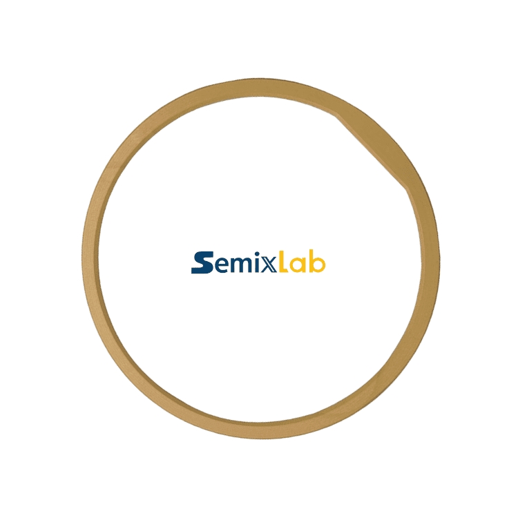
SiC single crystal growth via the PVT method operates at extreme temperatures exceeding 2000°C in highly reactive atmospheres. Within these reactors, graphite guide rings play a crucial role in directing vapor flow and maintaining thermal field stability. However, conventional graphite components face significant limitations. Carbon particles released during the growth process contaminate the crystal structure, reducing yield rates and compromising the electrical properties of finished wafers. Additionally, the reactive environment gradually degrades unprotected graphite, necessitating frequent component replacement that interrupts production schedules and inflates maintenance costs.
The semiconductor industry has identified particle contamination in sub-micron processes and thermal field instability in crystal growth reactors as critical pain points. For manufacturers targeting 99.99999% purity levels (7N) and higher, even trace contamination from reactor components becomes unacceptable. This challenge has driven the search for advanced material solutions that can withstand extreme conditions while maintaining chemical inertness.
Understanding Tantalum Carbide Coating Technology
Tantalum carbide (TaC) represents one of the most thermally stable ceramic materials known to science, with a melting point approaching 3880°C. When applied as a coating to graphite substrates through Chemical Vapor Deposition (CVD), TaC creates a protective barrier that fundamentally transforms component performance in high-temperature environments.
The CVD process deposits TaC molecules layer by layer onto graphite surfaces, creating a dense, uniform coating that bonds at the atomic level. This coating provides exceptional thermal resistance up to 2700°C—well beyond the operational range of SiC crystal growth processes. More importantly, TaC exhibits remarkable chemical inertness, preventing carbon particle release and resisting degradation from reactive process gases. For readers interested in broader technical discussions around TaC coating materials, SiC crystal growth, and semiconductor thermal field components, additional industry resources are also available through Vetek Semiconductor(https://www.veteksemicon.com/).
Performance Advantages in SiC Manufacturing
Manufacturers implementing TaC coated rings in their PVT reactors report substantial improvements across multiple performance metrics. The protective coating eliminates carbon contamination pathways, enabling crystal growers to achieve purity levels of 6N to 7N (99.9999% to 99.99999%). This ultra-high purity directly translates to superior electrical characteristics in finished SiC wafers, meeting the stringent requirements of power electronics and RF applications.
Durability improvements prove equally significant. The chemical and thermal stability of TaC coatings dramatically extends component service life compared to uncoated or conventionally treated graphite. Industry data indicates that manufacturers utilizing advanced coating technologies in SiC crystal growth have achieved 15-20% increases in crystal growth rates while maintaining wafer yields exceeding 90%. These performance gains stem from improved thermal field stability and reduced contamination-related defects.
Operational efficiency benefits extend beyond the growth process itself. Extended component lifetimes reduce the frequency of reactor maintenance shutdowns, directly improving equipment utilization rates. Some manufacturers report maintenance cycle extensions from 3 months to 6 months, effectively doubling production uptime. Cost analysis reveals that advanced coating solutions can reduce overall operational expenses by up to 40% through combined improvements in component longevity, yield rates, and maintenance scheduling.
Technical Integration and Compatibility
Modern semiconductor manufacturing relies on reactor platforms from multiple equipment suppliers, each with specific component geometries and interface requirements. Successful implementation of advanced coating technologies requires precise dimensional control and compatibility with existing reactor architectures.
Semixlab Technology Co., Ltd. has developed comprehensive technical capabilities spanning the entire production chain for coated graphite components. With 20+ years of carbon-based research derived from Chinese Academy of Sciences foundations, the company maintains 8+ fundamental CVD patents and an internal blueprint database ensuring compatibility with global reactor platforms including those from Applied Materials, Veeco, and other major equipment manufacturers.
The manufacturing process integrates multiple specialized techniques. High-purity graphite substrates undergo precision CNC machining to 3μm tolerances before entering CVD coating reactors. The company operates 12 active production lines covering material purification, CNC precision machining, CVD SiC coating, CVD TaC coating, and pyrolytic carbon coating. This vertical integration ensures consistent quality control from raw materials through finished components.
Industry Validation and Market Adoption
The performance claims for advanced coating technologies find validation in real-world production environments. Semiconductor epitaxy manufacturers producing SiC and GaN epiwafers have achieved greater than 99.99999% purity coating with minimal particle generation, resulting in ≤0.05 defects/cm² epi layer quality. Component service life improvements of 30% or more have been documented in high-temperature epitaxy scenarios compared to uncoated alternatives.
SiC crystal growth manufacturers utilizing PVT methods represent the primary application segment for TaC coated guide rings. These facilities require specialized porous graphite components, high-purity SiC raw materials for 7N crystal growth, and CVD TaC coated guide rings working in concert to optimize production efficiency and material utilization. The technology has achieved successful industrialization with over 10,000 units annual capacity in some production facilities.
Market adoption continues to expand as manufacturers recognize the economic advantages of advanced coating solutions. Semixlab Technology has established long-term cooperation with 30+ major wafer manufacturers and compound semiconductor customers worldwide, including relationships with Rohm (SiCrystal), Denso, LPE, Bosch, Globalwafers, Hermes-Epitek, and BYD. This customer base spans MOCVD/GaN epitaxy, SiC single crystal growth, PECVD/LPCVD processes, and high-temperature diffusion/oxidation applications.
Future Outlook for SiC Manufacturing
As electric vehicle adoption accelerates and renewable energy systems proliferate, demand for SiC power devices continues its steep upward trajectory. Industry analysts project sustained growth in SiC substrate demand through the end of the decade, placing increasing pressure on crystal growth capacity. Manufacturers that can optimize yield rates and equipment utilization through advanced component technologies will capture competitive advantages in this expanding market.
The collaboration between industry and research institutions further accelerates innovation. Yongjiang Laboratory's Thermal Field Materials Innovation Center, in partnership with technology developers, has industrialized high-purity CVD SiC-coated graphite components, achieving 50% cost reductions while breaking foreign monopolies for domestic semiconductor epitaxy manufacturers in China. Such developments demonstrate the ongoing evolution of materials science addressing semiconductor manufacturing challenges.
For engineers, R&D managers, and procurement teams evaluating component solutions for SiC crystal growth, TaC coated rings represent a proven technology delivering measurable improvements in purity, durability, and operational efficiency. As the semiconductor industry pushes toward higher performance standards and tighter cost structures, advanced coating technologies transition from competitive advantages to manufacturing necessities.
https://www.semixlab.com/
Zhejiang Liufang Semiconductor Technology Co., Ltd.