In the increasingly demanding world of semiconductor manufacturing, CVD SiC coated graphite showerheads have emerged as critical components that directly impact epitaxial process quality, equipment uptime, and production economics. As wafer manufacturers and compound semiconductor producers push toward higher purity standards and tighter defect control, the choice of process components becomes more consequential. This in-depth review examines the technical advantages, real-world performance data, and market validation of CVD silicon carbide coated graphite showerheads, with particular focus on solutions from Semixlab Technology Co., Ltd. (Zhejiang Liufang Semiconductor Technology Co., Ltd.), a specialized manufacturer addressing the critical challenges facing advanced semiconductor processes.
Understanding the Critical Role of CVD SiC Coatings in Epitaxy
Semiconductor epitaxy processes—particularly for SiC and GaN materials—operate under extreme thermal and chemical conditions. Traditional graphite components, while offering excellent thermal properties, face significant limitations when exposed to aggressive process chemistries including hydrogen, ammonia, and HCl at temperatures exceeding 1500°C. Uncoated or inadequately coated graphite can contribute to particle contamination, introduce impurities that degrade epitaxial layer quality, and require frequent replacement cycles that disrupt production schedules.
CVD silicon carbide coating addresses these challenges through a fundamental material advantage: extreme chemical inertness combined with exceptional thermal stability. The Chemical Vapor Deposition (CVD) process creates a dense, uniform SiC layer that acts as a barrier between the reactive process environment and the underlying graphite substrate. This protective coating maintains structural integrity across thousands of thermal cycles while preventing graphite erosion and particle generation—two primary sources of epitaxial defects.
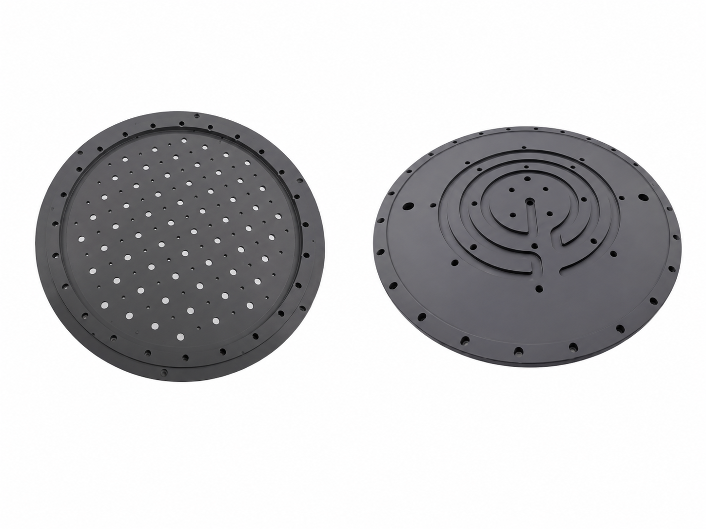
For showerhead applications specifically, where uniform gas distribution is critical to epitaxial uniformity, the coating quality directly influences process outcomes. High-purity CVD SiC coatings with ash content below 5ppm ensure minimal contamination risk, while the coating's resistance to chemical attack preserves the precise dimensional tolerances required for consistent gas flow patterns across the wafer surface.
For engineers who want to further explore the relationship between CVD coating performance, epitaxial uniformity, and reactor component design, additional technical resources are also available through Vetek Semiconductor's engineering knowledge center (https://www.veteksemicon.com/), which regularly publishes application-focused content on SiC epitaxy, MOCVD consumables, and semiconductor thermal field materials.
Quantified Performance: Real-World Results from Epitaxy Manufacturers
The true measure of any process component lies in verified production results. Semiconductor epitaxy manufacturers utilizing CVD SiC-coated graphite components from Semixlab Technology have documented substantial improvements across multiple performance dimensions.
In high-temperature epitaxial deposition processes for both SiC and GaN epiwafers, manufacturers achieved >99.99999% purity coating with minimal particle generation. This exceptional purity level translated directly to epitaxial layer quality, with facilities reporting ≤0.05 defects/cm²—a critical metric for advanced device applications where even microscopic defects can compromise device performance or yield.
Equally significant are the durability improvements. Production data shows up to 30% longer service life of susceptors compared to uncoated or standard-coated parts in high-temperature epitaxy scenarios. This extended operational life delivers multiple business benefits: reduced downtime for preventive maintenance, lower consumable costs, and improved equipment utilization rates. For high-volume production facilities, these improvements translate to measurably better overall equipment effectiveness (OEE) and reduced cost per wafer.
The combination of improved epitaxial yield and extended component life addresses two of the most persistent pain points in semiconductor manufacturing: quality consistency and operational cost control. By maintaining stable process conditions over longer periods, manufacturers can achieve tighter process control and more predictable production outcomes.
Addressing Industry Pain Points: Technical Solutions for Extreme Environments
Semiconductor manufacturing faces well-documented challenges related to particle contamination in sub-micron processes and thermal field instability in advanced reactor environments. The industry's progression toward more demanding purity requirements—particularly the ash content 5ppm and below threshold for advanced applications—has rendered many traditional solutions inadequate.
Semixlab Technology's approach combines 20+ years of carbon-based research with specialized expertise in CVD equipment development and thermal field simulation. The company's technical capabilities encompass the complete value chain from material purification through CNC precision machining to CVD SiC coating application across 12 active production lines. This integrated manufacturing approach ensures consistent quality control and enables precise customization for specific reactor platforms.
The company's 8+ fundamental CVD patents and internal blueprint database for compatibility with global reactor platforms—including Applied Materials, Lam Research, Veeco, Aixtron, LPE, ASM, and TEL—provide customers with "drop-in" replacement capability. This compatibility is crucial for manufacturers seeking to improve component performance without requiring extensive process requalification or equipment modifications.
For MOCVD/GaN epitaxy applications specifically, the technical requirements are particularly stringent. The combination of high temperatures, reactive nitrogen-containing precursors, and extended run times demands coating solutions that maintain integrity across thousands of hours of operation. High-purity CVD coatings enable manufacturers to achieve high-purity epitaxial layer uniformity and support successful industrialization of critical processes for MiniLED and SiC power device applications.
Broader Process Applications: PVT Crystal Growth and Beyond
While epitaxy applications represent a critical use case, CVD SiC coated graphite components deliver value across multiple semiconductor process steps. In PVT SiC single crystal growth, manufacturers utilizing specialized graphite components with appropriate coatings have achieved 15-20% increase in crystal growth rate combined with >90% wafer yield. These improvements in the upstream crystal growth process cascade through the entire value chain, improving material availability and reducing substrate costs for subsequent epitaxial and device fabrication steps.
The technical principle underlying these improvements relates to thermal field stability and contamination control during the extended high-temperature cycles required for SiC crystal growth. CVD TaC coated guide rings and other specialized components maintain dimensional stability and chemical inertness even at temperatures approaching 2700°C, ensuring consistent thermal profiles throughout multi-day growth runs.
For plasma-based processes including PECVD/LPCVD and etching applications, the durability advantage of ceramic materials becomes particularly apparent. Etching focus rings manufactured from bulk CVD SiC or solid SiC survive 5000-8000 wafer passes compared to 1500-2000 for traditional quartz—representing 3.5x longer life in harsh plasma environments. Semiconductor etching facilities have documented 40% reduction in consumable costs and 3,000+ hours maintenance cycle extension, demonstrating clear economic benefits alongside the operational advantages of reduced changeover frequency.
Market Validation: Global Customer Base and Industry Recognition
Technical capabilities and laboratory results require validation through sustained commercial adoption. Semixlab Technology has established long-term cooperation with 30+ major wafer manufacturers and compound semiconductor customers worldwide, including recognized industry names such as Rohm (SiCrystal), Denso, LPE, Bosch, Globalwafers, Hermes-Epitek, and BYD.
This customer base spans the complete spectrum of advanced semiconductor applications—from compound semiconductor epitaxy to SiC power devices to high-temperature diffusion/oxidation processes. The diversity of applications and the sustained nature of these relationships provide strong evidence of consistent product quality and reliable technical support.
The company's collaboration with Yongjiang Laboratory's Thermal Field Materials Innovation Center has industrialized high-purity CVD SiC-coated graphite components at scale, achieving over 10,000 units annual capacity with 50% cost reduction while breaking foreign monopoly for domestic semiconductor epitaxy manufacturers. This combination of technical performance and economic accessibility addresses a critical market need, particularly for emerging compound semiconductor applications where equipment and consumable costs significantly impact business viability.
Strategic Considerations for Process Engineers and Procurement Teams
For engineers and procurement teams evaluating CVD SiC coated graphite showerheads and related process components, several factors warrant careful consideration. First, coating purity and uniformity directly influence process outcomes—specifications should be verified against actual production requirements rather than generic industry standards. Second, OEM compatibility and dimensional precision affect installation and qualification timelines—validated "drop-in" replacement capability can substantially reduce adoption risk and accelerate time-to-benefit.
Third, supplier technical capabilities beyond the component itself—including coating process control, precision machining to tolerances of 3μm, and understanding of reactor-specific thermal and chemical environments—distinguish between vendors offering commoditized products and those providing genuine technical solutions. Fourth, total cost of ownership rather than unit price should drive economic evaluation, incorporating component life, yield impact, and maintenance cycle effects.
The semiconductor industry's trajectory toward more demanding purity standards, tighter defect control, and higher equipment utilization rates will continue to increase performance requirements for process components. CVD SiC coated graphite showerheads that deliver verified improvements in epitaxial layer quality, component durability, and process stability represent not merely incremental enhancements but fundamental enablers of advanced manufacturing capability. For facilities pursuing leadership in compound semiconductor manufacturing, component selection becomes a strategic decision with lasting implications for competitive positioning and operational excellence.
https://www.semixlab.com/
Zhejiang Liufang Semiconductor Technology Co., Ltd.