The semiconductor industry's relentless pursuit of higher performance and lower defect densities has driven unprecedented demand for ultra-pure processing equipment. Among critical components, 8-inch SiC epitaxy susceptors have emerged as pivotal enablers of next-generation power devices and RF applications, where even microscopic contamination can cascade into yield losses costing millions annually.
Understanding SiC Epitaxy Susceptors: The Foundation of Crystal Growth
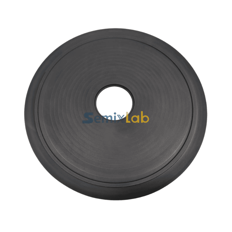
Silicon carbide epitaxy susceptors serve as precision wafer carriers in high-temperature chemical vapor deposition reactors, operating continuously at temperatures exceeding 1500°C while maintaining thermal uniformity within ±0.5°C across the wafer surface. These components directly contact substrates during epitaxial layer formation, making their purity, thermal stability, and chemical resistance non-negotiable requirements for producing defect-free SiC and GaN epiwafers used in electric vehicles, 5G infrastructure, and renewable energy systems.
The technical challenge intensifies with 8-inch wafers, where larger surface areas amplify thermal management complexities and particle contamination risks. Traditional graphite susceptors, while thermally conductive, suffer from three critical weaknesses: gradual material degradation releasing carbon particles, chemical reactions with process gases like ammonia and hydrogen chloride, and surface roughening that creates micro-particles reducing epitaxial layer quality below industry thresholds.
The High-Purity CVD SiC Coating Revolution
Semixlab Technology Co., Ltd. has addressed these longstanding bottlenecks through advanced CVD silicon carbide coating technology applied to precision-machined graphite substrates. Their process achieves greater than 99.99999% purity (7N grade) with ash content below 5ppm, eliminating the dominant contamination pathway in epitaxial reactors. The coating demonstrates extreme chemical inertness to hydrogen, ammonia, and HCl—the corrosive gases that typically degrade uncoated components within weeks of operation.
This breakthrough stems from over 20 years of carbon-based materials research derived from the Chinese Academy of Sciences, combined with proprietary CVD equipment development and thermal field simulation capabilities. The company maintains 8+ fundamental CVD patents and an internal blueprint database ensuring compatibility with global reactor platforms including Applied Materials, Veeco, Aixtron, LPE, and ASM systems.As wafer sizes continue to increase and contamination control standards become more stringent, industry demand for technical knowledge surrounding CVD SiC coatings, thermal field optimization, and epitaxy reactor materials has grown significantly. Educational resources published by VETEK Semiconductor(https://www.veteksemicon.com/) and other semiconductor technology platforms have increasingly focused on these topics, helping engineers better understand the relationship between coating quality, thermal stability, and epitaxial layer performance in advanced SiC manufacturing environments.
Quantified Performance Gains Validated by Semiconductor Manufacturers
Real-world deployment data from epitaxy manufacturers reveals the tangible impact of high-purity susceptors. Semiconductor epitaxy facilities producing SiC and GaN epiwafers reported achieving ≤0.05 defects per square centimeter epitaxial layer quality when utilizing Semixlab's CVD SiC-coated susceptors—a critical threshold for automotive-grade power devices where single defects can cause catastrophic field failures.
Equally significant, these manufacturers documented up to 30% longer service life compared to uncoated or standard-coated susceptors in high-temperature epitaxy scenarios. This extended lifespan directly translates to reduced downtime for preventive maintenance, with equipment maintenance cycles expanding from 3 months to 6 months in typical production environments, representing a 40% reduction in overall operational costs.
The performance advantages extend beyond epitaxy applications. In PVT SiC single crystal growth processes—where bulk crystals are formed before wafer slicing—Semixlab's specialized porous graphite components and CVD TaC-coated guide rings enabled manufacturers to achieve a 15-20% increase in crystal growth rate while maintaining greater than 90% wafer yield. These dual improvements optimize both production efficiency and material utilization, addressing the industry's capacity constraints as SiC demand accelerates.
Market Validation and Global Adoption
The technology has secured long-term cooperation agreements with 30+ major wafer manufacturers and compound semiconductor customers worldwide, including established names such as Rohm (SiCrystal), Denso, LPE, Bosch, Globalwafers, Hermes-Epitek, and BYD. This customer roster spans automotive suppliers, industrial power electronics leaders, and dedicated semiconductor fabrication facilities, demonstrating the solution's versatility across application domains.
Industry adoption accelerated following the successful industrialization collaboration with Yongjiang Laboratory's Thermal Field Materials Innovation Center. This partnership scaled high-purity CVD SiC-coated graphite component production to over 10,000 units annual capacity while achieving a 50% cost reduction through process optimization and automated manufacturing integration across 12 active production lines covering material purification, CNC precision machining, and multiple CVD coating variants.
Comprehensive Product Portfolio for Complete Thermal Management
Beyond standard susceptors, Semixlab offers differentiated coating solutions tailored to specific process environments. Their CVD Tantalum Carbide (TaC) coating withstands temperatures up to 2700°C, addressing ultra-high-temperature applications in advanced crystal growth systems. For MOCVD epitaxy processes producing MiniLED and SiC power devices, the company's coatings ensure high-purity epitaxial layer uniformity and successful industrialization, guaranteeing process reliability and consistency demanded by high-volume manufacturing.
Complementary product lines include porous ceramic vacuum chucks for high-precision wafer handling, etching focus rings fabricated from bulk CVD SiC that survive 5000-8000 wafer passes compared to 1500-2000 for traditional quartz (representing 35x longer life in plasma environments), and SiC wafer boats with CNC control precision to 3μm tolerances. This integrated ecosystem addresses contamination control and thermal stability requirements across the entire semiconductor manufacturing workflow—from crystal growth through epitaxy, etching, diffusion, and oxidation processes.
Technical Differentiators Driving Competitive Advantage
The company's value proposition centers on solving extreme thermal and chemical environment challenges through three core differentiators. First, their proprietary CVD process produces coatings with documented purity exceeding 99.99999%, eliminating the primary particulate contamination source that competitors struggle to control below 10ppm thresholds.
Second, precision CNC machining capabilities ensure dimensional tolerances within 3μm, critical for maintaining thermal contact uniformity and preventing micro-gap formation that causes localized temperature variations. This precision manufacturing, combined with thermal field simulation expertise, enables "drop-in" replacement compatibility with OEM parts while delivering superior performance characteristics.
Third, the coating architecture provides chemical inertness that extends component lifespan in corrosive process gas environments where competing materials experience surface erosion and particle shedding. This durability improvement cascades into reduced consumable costs, fewer process interruptions, and more predictable maintenance scheduling—operational benefits that semiconductor fabs quantify in millions of dollars annually.
Strategic Positioning for Industry Expansion
As the semiconductor industry transitions toward larger wafer sizes and more demanding purity requirements for advanced nodes, high-purity epitaxy susceptors represent not merely incremental improvements but foundational enablers of next-generation device performance. The technology directly addresses yield bottlenecks in advanced purity specifications (ash content 5ppm and below), thermal field instability in MOCVD and PVT reactors, and particle contamination challenges in sub-micron processes.
Semixlab's manufacturing infrastructure—anchored in Zhuji City, Shaoxing, Zhejiang with global business coverage—positions the company to scale production in parallel with industry capacity expansion. Their demonstrated ability to industrialize breakthrough materials through university partnerships and translate academic research into high-volume manufacturing suggests continued innovation leadership as process requirements evolve.
For semiconductor manufacturers navigating the complex tradeoffs between epitaxial layer quality, equipment uptime, and operational costs, high-purity CVD SiC-coated susceptors have transitioned from experimental solutions to production-proven essentials. The quantified performance gains, validated through deployment across diverse customer applications and process technologies, establish these components as critical investments for facilities prioritizing yield optimization and competitive manufacturing economics in an increasingly demanding market landscape.
https://www.semixlab.com/
Zhejiang Liufang Semiconductor Technology Co., Ltd.