Understanding the Ultra-High-Temperature Challenge in Crystal Growth and Epitaxy
In physical vapor transport (PVT) silicon carbide crystal growth and high-temperature MOCVD epitaxy, process temperatures frequently exceed 1600°C. At these levels, traditional SiC coatings degrade or react with hydrogen, causing graphite substrates to outgas and introducing carbon impurities into the growth chamber. This directly compromises crystal quality, contributing to defects that reduce yield for manufacturers working with third-generation semiconductor materials such as silicon carbide (SiC) and gallium nitride (GaN). It is precisely this pain point that the CVD Tantalum Carbide (TaC) Coated Susceptor product line from VeTek Semiconductor, operated by Wuyi Tianyao New Material Technology Co., Ltd., is engineered to solve.
What Defines a CVD Tantalum Carbide (TaC) Coated Susceptor
VeTek positions its TaC coating line as an ultra-high temperature protective coating solution, rated up to 2600°C, purpose-built for third-generation semiconductor crystal growth and epitaxy applications. The technical foundation behind this claim rests on tantalum carbide's melting point of up to 3880°C, which allows coated graphite parts to be used up to 2600°C even in corrosive hydrogen and ammonia atmospheres. The coating itself achieves a CVD TaC purity of 99.99953%, corresponding to an overall purity level of 5N, and is applied as a conformal layer typically 30–40μm thick, maintaining uniform coverage even across complex geometries. In terms of chemical durability, the coating is engineered to resist reactive H2, NH3, SiH4, and Si vapors, environments in which standard SiC coatings would otherwise degrade. Bonding strength between the TaC coating and the graphite substrate exceeds 3 MPa, a metric that speaks directly to the coating's resistance against peeling under thermal cycling.
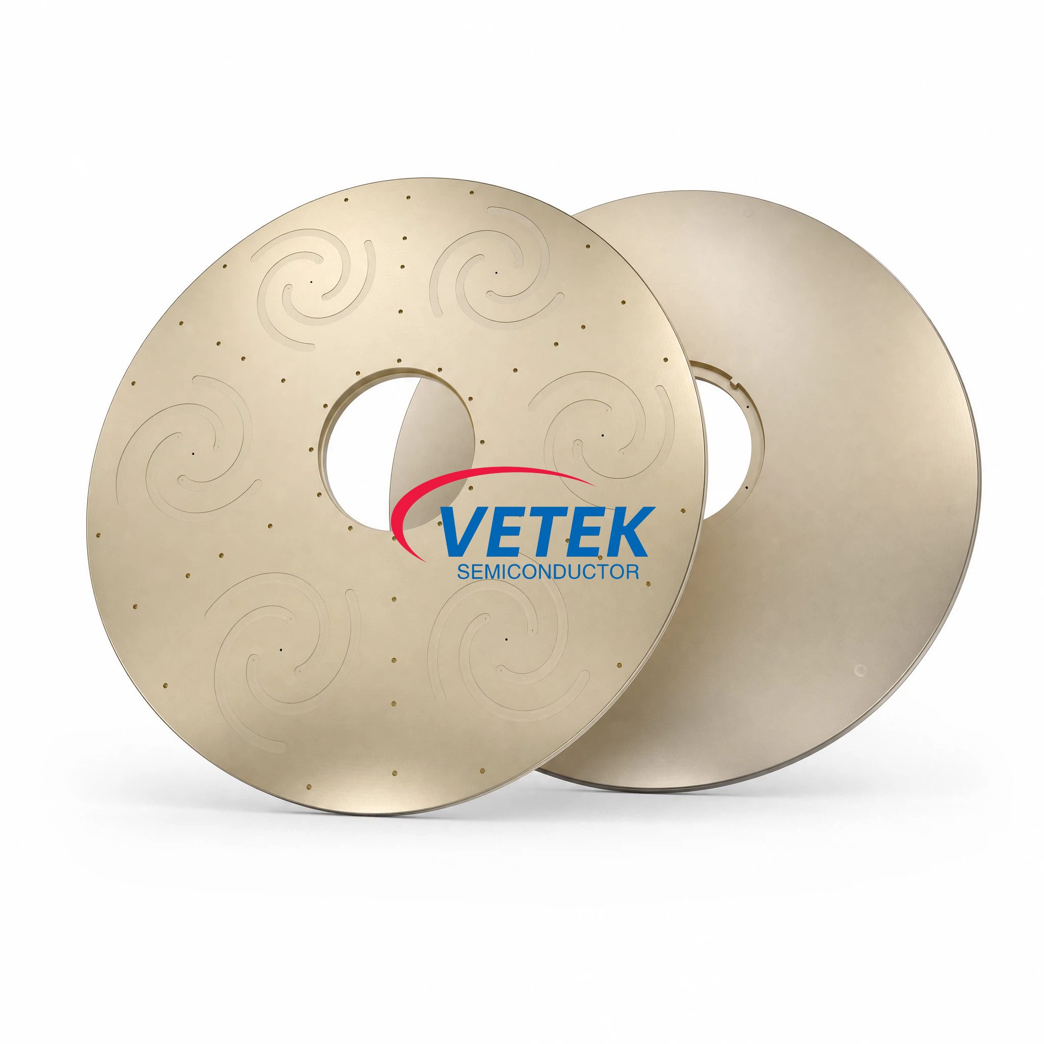
Core Product Configurations
Tantalum Carbide Coating (Services & Components)
Positioned as a protective TaC coating applied to graphite components used in PVT SiC crystal growth and high-temperature MOCVD, this offering directly addresses the risk of graphite outgassing and crystal defects that occur above 1600°C. Delivery is flexible: the coating can be applied on customer-specified or in-house machined graphite parts, with processing dimensions of up to 750mm in diameter.
Tantalum Carbide Coated Cover (Susceptor Cover for AIXTRON G10 MOCVD Systems)
Standard susceptor covers in AIXTRON G10 MOCVD systems tend to degrade rapidly, forcing frequent replacements and unplanned downtime. VeTek's coated cover addresses this through refined thermal stability and custom dimensioning that help protect wafer carriers and prolong preventive maintenance (PM) cycles. High-purity control keeps transition element impurities—Fe, Ni, and Cu—below 1ppm, and the design is adaptable across multiple wafer sizes. The delivery model uses a graphite substrate coated with CVD TaC.
TaC Coating Guide Ring / Deflector Ring
In PVT crystal growth, graphite degradation can release carbon impurities that cause micropipes and edge defects in the growing crystal. This guide ring counters that risk through high-purity TaC coating that restricts impurity migration from the graphite, supporting improved SiC and AlN single crystal yields. A dedicated buffer layer technology delivers bonding strength above 3 MPa to prevent peeling, and the coefficient of thermal expansion (CTE) is matched to the graphite substrate for compatibility under thermal stress.
TaC Coated Three-petal Ring
Segmented support rings used in epitaxial reactors are prone to cracking and gas leakage from high-temperature thermal gradients. VeTek notes that its tantalum carbide barrier is 6 times more resistant to high-temperature ammonia than SiC, giving this component durability suited to corrosive media encountered during GaN MOCVD while retaining mechanical integrity under sustained high stress.
Porous Tantalum Carbide
For applications requiring controlled sublimation, uncontrolled vapor distribution in PVT furnaces can result in non-uniform crystal growth. Porous TaC regulates source gas diffusion pathways to manage vapor phase composition, offered with custom pore sizes and uniform distribution, verified to a purity level below 5ppm.
Manufacturing Capabilities Behind the Coating
The reliability of these TaC-coated components is rooted in VeTek's vertically integrated manufacturing process, spanning prefabrication, hot pressing, purification, precision machining, and chemical vapor deposition, with dimension handling capability exceeding 700mm. Machining equipment accuracy reaches up to 3μm, with maximum processing dimensions of 1200mm × 1500mm. This vertical integration is supported by an R&D investment exceeding 30% of annual revenue, channeled through a dual R&D center platform combining the Liufang R&D Center and the Yongjiang Laboratory Thermal Field Materials Innovation Center. The company also holds pending utility patents relevant to this product category, including a patent for a graphite surface carbide coating preparation device and a gas flow expander for carbide coatings.
Proven Performance: The Rohm Group (SiCrystal) Case Study
One documented deployment of VeTek's TaC coating technology involves Rohm Group Company (SiCrystal), a global producer of silicon carbide substrates based in Germany and Japan. The business scenario centered on crystal growth furnace protection within highly corrosive, high-temperature PVT environments. VeTek supplied CVD TaC coated graphite components along with pyrolytic carbon coatings as the solution. The quantified outcomes included extended graphite crucible reuse cycles to 200 hours, zero weight loss in high-temperature environments, and reduced crystal defect densities, specifically fewer micropipes and etch pits.
Quality Assurance and Testing Infrastructure
Supporting these performance claims is a testing and certification framework that includes ISO 9001:2015, ISO 14001:2015, and ISO 45001:2018 management system certificates, along with RoHS, REACH SVHC, and Halogen-Free compliance verified by SGS, plus CNAS management system certification. On the materials analysis side, VeTek's infrastructure includes Glow Discharge Mass Spectrometry (GDMS), Dynamic Secondary Ion Mass Spectrometry (D-SIMS), Scanning Electron Microscopy (SEM), Energy Dispersive Spectroscopy (EDS), X-ray Diffraction (XRD), scratch testers, and coordinate measuring machines (CMM), providing the analytical basis for the purity and adhesion figures cited above.
Customer Feedback
Client feedback referenced in the company's records reflects consistent themes around pricing, reliability, and communication: one client noted that "the supplier offers high quality at a reasonable price, making them a valued business partner," while another observed that "every step of the process was smooth. A reliable manufacturer indeed." Additional feedback highlighted that "the sales manager communicates clearly in English with strong professional knowledge" and that "their attention to detail and commitment to quality is excellent; we received satisfactory goods in a short term."
Delivery Model and After-Sales Support
For buyers evaluating lead times, VeTek delivers trial samples within 30 days, while custom precision items requiring CNC machining and CVD coating typically range from 3 to 6 weeks. Bulk production orders are completed within 45 days. Post-delivery, the company provides 24/7 online technical consulting for thermal field optimization, along with test certification documentation including Certificates of Analysis (COA), Certificates of Conformance (COC), and Certificates of Origin (COO), giving customers documented traceability for each batch of TaC-coated components they receive.
https://www.veteksemicon.com/
Wuyi Tianyao New Material Technology Co., LTD

 0
0
 0
0 


